BUZ 73A H
SIPMOS ® Power Transistor
• N channel
• Enhancement mode
• Avalanche-rated
. Halogen-free according to IEC61249-2-21
Pin 1
Pin 2
G
Pin 3
D
Type
VDS
ID
RDS(on)
Package
Pb-free
BUZ 73 A
200 V
5.5 A
0.6 Ω
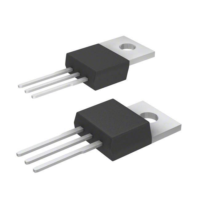
PG-TO-220-3
yes
S
Maximum Ratings
Parameter
Symbol
Continuous drain current
ID
TC = 37 ˚C
Pulsed drain current
Values
Unit
A
5.5
IDpuls
TC = 25 ˚C
22
Avalanche current,limited by Tjmax
IAR
7
Avalanche energy,periodic limited by Tjmax
E AR
6.5
Avalanche energy, single pulse
E AS
mJ
ID = 7 A, VDD = 50 V, RGS = 25 Ω
L = 3.67 mH, Tj = 25 ˚C
120
Gate source voltage
VGS
Power dissipation
Ptot
TC = 25 ˚C
± 20
W
40
Operating temperature
Tj
-55 ... + 150
Storage temperature
Tstg
-55 ... + 150
Thermal resistance, chip case
RthJC
≤ 3.1
Thermal resistance, chip to ambient
RthJA
75
DIN humidity category, DIN 40 040
˚C
K/W
E
55 / 150 / 56
IEC climatic category, DIN IEC 68-1
Rev. 2.4
V
Page 1
2009-11-10
�BUZ 73A H
Electrical Characteristics, at Tj = 25˚C, unless otherwise specified
Parameter
Symbol
Values
min.
typ.
Unit
max.
Static Characteristics
Drain- source breakdown voltage
V (BR)DSS
VGS = 0 V, ID = 0.25 mA, Tj = 25 ˚C
Gate threshold voltage
200
-
-
V GS(th)
V GS=VDS, ID = 1 mA
Zero gate voltage drain current
V
2.1
3
4
IDSS
µA
VDS = 200 V, V GS = 0 V, Tj = 25 ˚C
-
0.1
1
VDS = 200 V, V GS = 0 V, Tj = 125 ˚C
-
10
100
Gate-source leakage current
IGSS
V GS = 20 V, VDS = 0 V
Drain-Source on-resistance
-
10
100
Ω
RDS(on)
V GS = 10 V, ID = 4.5 A
Rev. 2.4
nA
-
Page 2
0.5
0.6
2009-11-10
�BUZ 73A H
Electrical Characteristics, at Tj = 25˚C, unless otherwise specified
Parameter
Symbol
Values
min.
typ.
Unit
max.
Dynamic Characteristics
Transconductance
gfs
VDS≥ 2 * ID * RDS(on)max, ID = 4.5 A
Input capacitance
3
pF
-
400
530
-
85
130
-
45
70
Crss
V GS = 0 V, V DS = 25 V, f = 1 MHz
Turn-on delay time
-
Coss
V GS = 0 V, V DS = 25 V, f = 1 MHz
Reverse transfer capacitance
4.2
Ciss
V GS = 0 V, V DS = 25 V, f = 1 MHz
Output capacitance
S
td(on)
ns
V DD = 30 V, VGS = 10 V, ID = 3 A
RGS = 50 Ω
Rise time
-
10
15
-
40
60
-
55
75
-
30
40
tr
V DD = 30 V, VGS = 10 V, ID = 3 A
RGS = 50 Ω
Turn-off delay time
td(off)
V DD = 30 V, VGS = 10 V, ID = 3 A
RGS = 50 Ω
Fall time
tf
V DD = 30 V, VGS = 10 V, ID = 3 A
RGS = 50 Ω
Rev. 2.4
Page 3
2009-11-10
�BUZ 73A H
Electrical Characteristics, at Tj = 25˚C, unless otherwise specified
Parameter
Symbol
Values
min.
typ.
Unit
max.
Reverse Diode
Inverse diode continuous forward current
IS
TC = 25 ˚C
Inverse diode direct current,pulsed
-
-
22
V
1.3
1.7
trr
ns
-
200
-
Qrr
V R = 100 V, IF=lS, diF/dt = 100 A/µs
Rev. 2.4
5.5
-
V R = 100 V, IF=lS, diF/dt = 100 A/µs
Reverse recovery charge
-
V SD
VGS = 0 V, IF = 14 A
Reverse recovery time
ISM
TC = 25 ˚C
Inverse diode forward voltage
A
µC
-
Page 4
0.6
-
2009-11-10
�BUZ 73A H
Drain current
ID = ƒ(TC)
parameter: VGS ≥ 10 V
Power dissipation
Ptot = ƒ(TC)
6.0
45
A
W
5.0
Ptot
ID
35
4.5
4.0
30
3.5
25
3.0
20
2.5
15
2.0
1.5
10
1.0
5
0.5
0
0
0.0
20
40
60
80
100
120
˚C
0
160
20
40
60
80
100
120
TC
Safe operating area
ID = ƒ(VDS)
parameter: D = 0.01, TC = 25˚C
˚C
160
TC
Transient thermal impedance
Zth JC = ƒ(tp)
parameter: D = tp / T
10 2
10 1
K/W
A
t = 36.0µs
p
ID
ZthJC
/I
D
100 µs
R
DS
(o
n)
=V
DS
10 1
10 0
10 -1
1 ms
D = 0.50
0.20
10 0
0.10
10 ms
0.05
10 -2
0.02
0.01
single pulse
DC
10 -1
0
10
10
1
10
2
10 -3
-7
10
V
VDS
Rev. 2.4
10
-6
10
-5
10
-4
10
-3
10
-2
-1
10 s 10
0
tp
Page 5
2009-11-10
�BUZ 73A H
Typ. output characteristics
ID = ƒ(VDS)
parameter: tp = 80 µs
13
Typ. drain-source on-resistance
RDS (on) = ƒ(ID)
parameter: VGS
1.8
Ptot = 40W
kj i h g
ID
VGS [V]
10
e
a
4.0
b
4.5
c
5.0
d
5.5
8
e
6.0
7
d f
6.5
g
7.0
h
7.5
i
8.0
j
9.0
9
6
5
c
4
RDS (on)
l
1.4
1.0
0.8
e
f
g
h
i j
0.6
20.0
k
0.4
b
2
0
0
VGS [V] =
0.2
a
1
d
1.2
k 10.0
3
c
Ω
f
11
b
a
l
A
a
4.5
4.0
b
5.0
c
5.5
d
6.0
e
f
6.5 7.0
g
7.5
h
i
j
k
8.0 9.0 10.0 20.0
0.0
2
4
6
8
10
12
V
16
0
2
4
6
8
A
VDS
Typ. transfer characteristics ID = f (V GS)
Typ. forward transconductance gfs = f (ID)
parameter: tp = 80 µs
parameter: tp = 80 µs,
VDS≥2 x ID x RDS(on)max
V DS≥2 x ID x RDS(on)max
13
6.0
A
S
11
ID
11
ID
5.0
gfs
10
9
4.5
4.0
8
3.5
7
3.0
6
2.5
5
2.0
4
1.5
3
2
1.0
1
0.5
0
0.0
0
1
2
3
4
5
6
7
8
V
10
0
VGS
Rev. 2.4
2
4
6
8
A
12
ID
Page 6
2009-11-10
�BUZ 73A H
Gate threshold voltage
VGS (th) = ƒ(Tj )
parameter: VGS = VDS, ID = 1 mA
Drain-source on-resistance
RDS (on) = ƒ(Tj )
parameter: ID = 4.5 A, VGS = 10 V
4.6
1.9
Ω
V
98%
4.0
1.6
VGS(th)
RDS (on)
3.6
1.4
typ
3.2
1.2
2.8
1.0
2.4
98%
0.8
2%
2.0
typ
1.6
0.6
1.2
0.4
0.8
0.2
0.4
0.0
-60
-20
20
60
100
˚C
0.0
-60
160
-20
20
60
100
Typ. capacitances
˚C
160
Tj
Tj
Forward characteristics of reverse diode
IF = ƒ(VSD)
parameter: Tj , tp = 80 µs
C = f (VDS)
parameter:VGS = 0V, f = 1MHz
10 1
10 2
nF
A
IF
C
10 0
10 1
Ciss
10 -1
10 0
Tj = 25 ˚C typ
Coss
Tj = 150 ˚C typ
Crss
Tj = 25 ˚C (98%)
Tj = 150 ˚C (98%)
10 -2
0
5
10
15
20
25
30
V
40
10 -1
0.0
VDS
Rev. 2.4
0.4
0.8
1.2
1.6
2.0
2.4
V
3.0
VSD
Page 7
2009-11-10
�BUZ 73A H
Avalanche energy EAS = ƒ(Tj)
parameter: ID = 7 A, VDD = 50 V
RGS = 25 Ω, L = 3.67 mH
Typ. gate charge
VGS = ƒ(QGate)
parameter: ID puls = 14 A
130
16
mJ
V
110
EAS
VGS
100
12
90
10
80
0,8 VDS max
0,2 VDS max
70
8
60
50
6
40
4
30
20
2
10
0
20
0
40
60
80
100
120
˚C
160
Tj
0
4
8
12
16
20
24
28
32 nC 38
Q Gate
Drain-source breakdown voltage
V(BR)DSS = ƒ(Tj)
240
V
230
V(BR)DSS
225
220
215
210
205
200
195
190
185
180
-60
-20
20
60
100
˚C
160
Tj
Rev. 2.4
Page 8
2009-11-10
�BUZ 73A H
Package Drawing: TO220-3
Rev. 2.4
Page 9
2009-11-10
�BUZ 73A H
Published by
Infineon Technologies AG
81726 Munich, Germany
© 2009 Infineon Technologies AG
All Rights Reserved.
Legal Disclaimer
The information given in this document shall in no event be regarded as a guarantee of
conditions or characteristics. With respect to any examples or hints given herein, any typical
values stated herein and/or any information regarding the application of the device,
Infineon Technologies hereby disclaims any and all warranties and liabilities of any kind,
including without limitation, warranties of non-infringement of intellectual property rights
of any third party.
Information
For further information on technology, delivery terms and conditions and prices, please
contact the nearest Infineon Technologies Office
(www.infineon.com).
Warnings
Due to technical requirements, components may contain dangerous substances. For information
on the types in question, please contact the nearest Infineon Technologies Office.
Infineon Technologies components may be used in life-support devices or systems only with
the express written approval of Infineon Technologies, if a failure of such components can
reasonably be expected to cause the failure of that life-support device or system or to affect
the safety or effectiveness of that device or system. Life support devices or systems are
intended to be implanted in the human body or to support and/or maintain and sustain
and/or protect human life. If they fail, it is reasonable to assume that the health of the user
or other persons may be endangered.
Rev. 2.4
Page 10
2009-11-10
�


 工商网监
湘ICP备2023018690号
工商网监
湘ICP备2023018690号
